Temperature Sensor with 10-bit SAR Analog-to-Digital Converter
A project for ECE 547 "VLSI Design" - Fall Semester 2010
Department of Electrical and Computer Engineering
University of Maine
Designed by: Steven Pesut
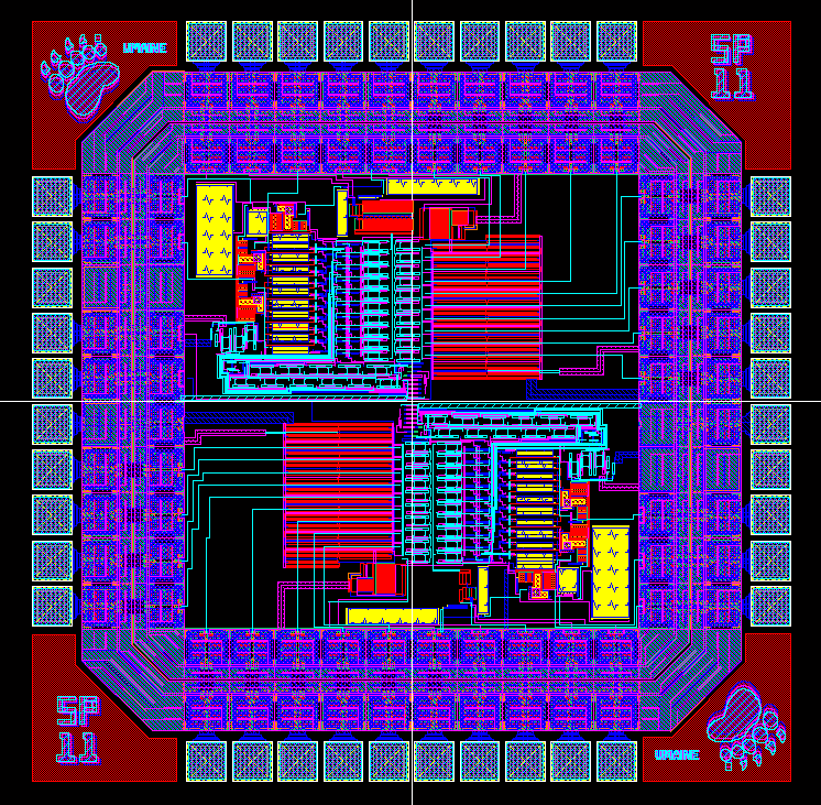
The design consists of three main stages. First, there is a circuit that is sensitive to ambient temperature changes. An amplification stage then turns the output of the sensing circuit into a usable signal. Lastly, the amplified signal is fed into a 10-bit analog-to-digital converter. The ADC is a Successive Approximation Register (SAR) which utilizes an R-2R Digital-to-Analog converter to generate the digital outputs. Simulations show the sensor to have a resolution of approximately +.5 oC with each conversion taking approximately a minimum of 550 μs and a maximum of 1.05 ms. Test and verification procedures are outlined and described. Both a low and high current design are implemented on the chip.
The project report contains a description of the project and details of the design and layout.