Sequence Generator
A project for ECE 547 "VLSI Design" - Fall Semester 2004
Department of Electrical and Computer Engineering
University of Maine
Designed by: Roman Shugayev
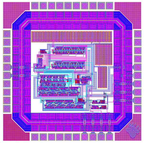
The ECE 547 VLSI design project consists of 128 bit sequence generator. Upon receiving an external enable signal the chip starts the process that results in a delayed 128 bit sequence appearing at the output of the chip. The sequential data and the duration of the delay are determined by the data stored in the ROM circuit of the sequence generator.
The project report contains a project description with design and layout considerations.