Low Power ROM, Decoder and Transmitter
A project for ECE 547 "VLSI Design" - Fall Semester 2011
Department of Electrical and Computer Engineering
University of Maine
Designed by: Jamie Reinhold
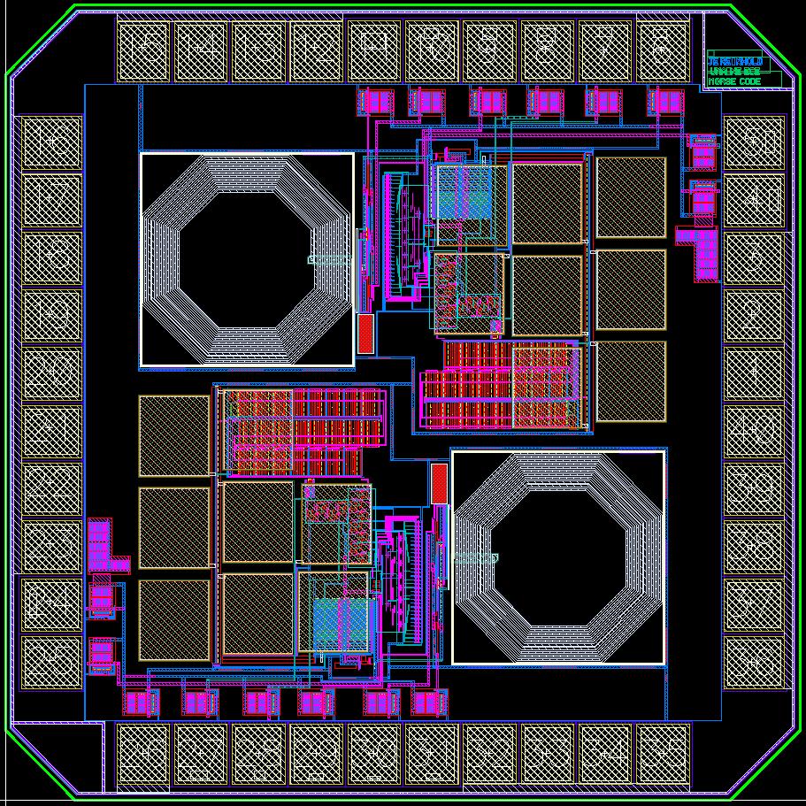
The design, simulation and layout of a low power‘UMAINE ECE’ Morse code Read Only Memory and transmitter are described. The chip uses a band-gap reference circuit to convert a voltage stored onto a capacitor, to a DC power supply that is insensitive to temperature. The band-gap reference powers a variety of clocks used in the timing for 32x4-bit ROM and 32-bit multiplexer; all based from a voltage-controlled oscillator. The output of the ROM and multiplexer is the Morse code representation of UMAINE ECE, which is transmitted by a 433MHz sinusoidal oscillator and off-chip antennae. Logic 1 is represented by oscillation and Logic 0 is no oscillation. Simulations show less than +10mV variation around 1.185V in the band-gap reference output from -50?C to 125?C with a charge on the capacitor ranging from 1.7V to 2.6V. The output of the overall circuit is a 325mV peak-to-peak sinusoid that oscillates at 433MHz (ISM-band frequency), where each character in the Morse code has a 50ms pulse width. Test and verification procedures are outlined and described.
The project report contains a description of the project and details of the design and layout.